As it has done in the past, Samsung is dual sourcing the image sensors for the Galaxy S9 andS9+ – depending on where you buy yours, it may have a Sony-designed IMX345 or a Samsung-designed S5K2L3 ISOCELL Fast. TechInsights has examined both sensors at a microscopic level and found them to have a different design.
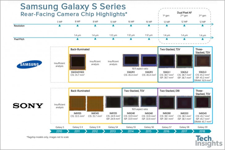
Both sensors have a 3-layer stacked design – a CMOS sensor with the image pixels, another for the image signal processor (ISP) and finally a DRAM chip for those coveted 960fps videos. But the organization is different.
Sony’s IMX345 is very similar to the IMX400 introduced with the Xperia XZs a year ago. It puts the DRAM in between the CMOS sensor and the ISP logic.
The Samsung S5K2L3 on the other hand looks like a traditional 2-layer sensor with a CMOS bonded to an ISP but it now as a DRAM chip connected to the bottom. Specifically, a LPDDR4 chip measuring 3.17 x 5.33 mm (16.9 mm²).
We even got an interesting timeline showing that Samsung has been catching up to Sony. Sony was the first to introduce a 2-layer design in 2014, followed by Samsung’s version in 2016. Then Sony made a 3-layer sensor last year and Samsung made one this year.

You can follow the source link for more intricate details on the image sensors. For example, Sony experimented with a copper direct bond interconnect between the CMOS and the ISP layers in the 2014-2016 period (this allows for higher density chips compared to the classic approach used in the 2017-2018 image sensors).
PS. You can use AIDA64 to check which sensor is in your Galaxy S9, just look at the Camera ID.


0 comments:
Post a Comment